Spintronics has attracted considerable attention because of its high performance in data storage and transfer. By manipulating the spin degree of freedom of electrons, spintronics can transmit information using spins rather than charges. Spintronics evolved through three stages: giant magnetoresistance (GMR), tunneling magnetoresistance (TMR), and semiconductor spintronics. The GMR and TMR devices are both all-metal spin devices using ferromagnetic metals, which pose a challenge for the integration of spin devices.1 Therefore, the exploration of semiconductor spintronics flourishes. Creating semiconductor spintronic devices begins with generating spin currents, which can be realized by spin−orbit coupling (SOC).2 Resulting from a magnetic field B ∼ E × p in the rest frame of electrons, SOC can remove the spin degeneracy of electronic bands without an external magnetic field, where the intrinsic electric field E is the gradient of the crystalline potential.
SOC exists in noncentrosymmetric structures and mainly consists of two types: the Rashba effect induced by the structure inversion asymmetry (SIA)3,4 and the Dresselhaus effect induced by the bulk inversion asymmetry (BIA).2 The Rashba effect and Dresselhaus effect were discovered in wurtzite5 and zinc-blende2 semiconductors, respectively. Further research by Bychkov and Rashba demonstrated that the Rashba effect also occurs in quasi-2D systems.3 Over the past few decades, the Rashba effect and Dresselhaus effect have been observed in various systems, such as 2D semiconductors, heterostructures, metal surfaces, 3D bulk materials, and quantum wells.
2D semiconductors are promising SOC materials. On the one hand, semiconductors are promising candidates for spintronics as mentioned above. On the other hand, 2D materials are superior to 3D materials for two main reasons: In 3D Rashba materials, maintaining bulk properties requires sufficient thickness, which limits the size of spintronic devices. In 2D Rashba materials, the momentum offset (kR) of the Rashba states lacks z components in reciprocal space, which satisfies the requirement for spin field effect transistors that kR should be perpendicular to the direction of the built-in electric field (z-direction).26 The advent of graphene in 200427 accelerated the development of other 2D materials, including phosphorene, transition-metal dichalcogenides (TMDs), boron nitride (BN), and silicene. But these 2D nonpolar semiconductors lack the intrinsic Rashba effect, such as phosphorene and transitionmetal dichalcogenides (TMDs).28,29 Although the external electric field12 and interfacial effect30 can break the out-of-plane symmetry in nonpolar structures and thus induce the Rashba effect, 2D polar semiconductors with the intrinsic Rashba effect merit further investigation. However, 2D SOC semiconductors have not been comprehensively summarized in previous studies.
In this theoretical Perspective, we review SOC including the Rashba effect and Dresselhaus effect in 2D semiconductors. We start with an overview of the Hamiltonian model and characterization methods of the Rashba effect and Dresselhaus effect. Then, we summarize 2D SOC semiconductors, such as AB binary monolayers, Janus monolayers (especially for MXY Janus monolayers), 2D perovskites, and so forth. We also review manipulating methods of the Rashba effect, including external electric field, strain engineering, charge doping, interlayer interactions, proximity effect of substrates, and external magnetic field. Then, we briefly summarize the applications of SOC, including the generation, detection, and manipulation of spin currents in spin Hall effect transistors and spin field effect transistors. Finally, we provide an outlook on the SOC effect in low-dimensional semiconductors, including the nonlinear SOC Hamiltonian, 2D ferroelectric SOC semiconductors, and 1D SOC.
This theoretical Perspective reviews spin−orbit coupling (SOC), including the Rashba effect and Dresselhaus effect, in two-dimensional (2D) semiconductors. We first introduce the origin of the Rashba effect and Dresselhaus effect using the Hamiltonian models; we then summarize 2D Rashba semiconductors predicted by first-principles density functional theory (DFT) calculations, including AB binary monolayers, Janus monolayers, 2D perovskites, and so on. We also review various manipulating techniques of the Rashba effect on 2D semiconductors, such as external electric field, strain engineering, charge doping, interlayer interactions, proximity effect of substrates, and external magnetic field. We then briefly summarize the applications of SOC, including the generation, detection, and manipulation of spin currents in spin Hall effect transistors and spin field effect transistors.
Finally, we conclude this Perspective and propose three promising research fields of SOC in low-dimensional semiconductors, including the nonlinear SOC Hamiltonian model, 2D ferroelectric SOC semiconductors, and 1D Rashba model and semiconductors. This theoretical Perspective enriches the fundamental understanding of SOC in 2D semiconductors and will help in the design of new types of spintronic devices in future experiments.
Figure 2. (a) 3D band structure without SOC is 2-fold degenerate in spin. 3D band structures with (b) the Rashba effect and (c) Dresselhaus effect have band splitting and special spin textures. (d) 2D schematic illustration of the Rashba effect. ER represents the energy difference between the vertex of the energy curve and the degenerate energy at the high-symmetry point, and kR represents the corresponding momentum offset. Spin textures of (e) the Rashba effect and (f) Dresselhaus effect. Arrows indicate in-plane spin directions. Red (blue) represents the positive (negative) spin component along the y axis.
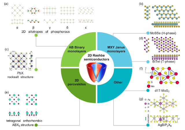
Figure 3. Schematic diagram of 2D Rashba semiconductors. (a) Top (upper row) and side (lower row) views of 2D binary phosphorene-type GeTe monolayers with α, β, γ, δ, and ϵ phases, where only the β-phase is suitable Rashba material. The green and brown balls represent two different atoms. Reprinted from ref 7. Copyright 2021 American Chemical Society. (b) Top (upper panel) and side (lower panel) views of H-phase MoSSe monolayer. Reprinted from ref 43. Copyright 2019 American Chemical Society. (c) (Left) top and (right) side views of square buckled PbX (X = S, Se, Te) monolayer. Blue and orange arrows denote vectors connecting Pb atom and its first- and second-nearest neighbors, respectively. Reprinted with permission from ref 8. Copyright 2017 American Physical Society. (d) Top (upper panel) and side (lower panel) views of T-phase BiTeI monolayer. Reprinted from ref 43. Copyright 2019 American Chemical Society. (e) Top (upper row) and side (lower row) views of 2D polar CsPbI3 structures from 3D tetragonal and orthorhombic bulk structures. The green, gray, and purple and balls represent Cs, Pb, and I atoms, respectively. 2D polar perovskites with ABX3 (A = Cs+, Rb+; B = Pb2+, Sn2+; X = Cl, Br, I) have similar structures. Reprinted from ref 16. Copyright 2021 American Chemical Society. (f) Structure of d1T-MoS2. Green arrows represent displacement vectors of the d1T phase with respect to the centrosymmetric 1T phase. Reprinted with permission from ref 44. Copyright 2014 American Physical Society. (g) Top (upper panel) and side (lower panel) views of ferroelectric AgBiP2X6 (X = S, Se, and Te) monolayer. Reprinted with permission from ref 17. Copyright 2020 American Physical Society.
Figure 4. (a) Electric field dependence of the linear Rashba constants (αR) of the six MX2 (M = Mo, W; X, Y = S, Se, Te) monolayers. Reprinted from ref 12. Copyright 2017 American Physical Society. (b) Calculated Rashba constants (αKR) around the Γ point along the Γ-K direction under different biaxial in-plane strains for Janus MXY monolayers (M = Mo, W; X, Y = S, Se, Te; X ≠ Y). Reprinted with permission from ref 10. Copyright 2018 American Physical Society. (c) Calculated Rashba constants (αKR) around the Γ point along the Γ-K direction under the external electric field for Janus MXY monolayers (M = Mo, W; X, Y = S, Se, Te; X ≠ Y). Reprinted with permission from ref 10. Copyright 2018 American Physical Society. (d) Calculated Rashba constants (αR) under different uniaxial in-plane strains for AlBi monolayer. Reprinted from ref 7. Copyright 2021 American Chemical Society.
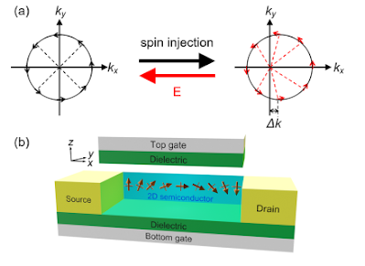
Figure 5. (a) Schematic illustration of the Rashba−Edelstein effect and inverse Rashba−Edelstein effect. In the Fermi contours with the Rashba effect, spins are perpendicular to the momentum. (Left to right, spin-tocharge conversion) When injecting the spin current polarized along the y direction, the charge current is generated by the spin texture shifts Δk along the x direction due to the spin-momentum locking injections. (Right to left, charge-to-spin conversion) When applying the electric field along the x direction, the Fermi surface is displaced by Δk and spins tilt, generating spin currents along the y direction. (b) A spin FET based on a 2D semiconductor.


